Liquid Crystal Displays (LCDs) have revolutionized visual technology, becoming ubiquitous in everything from smartphones to large-scale digital signage. Their success stems from a sophisticated combination of material science, electrical engineering, and precision manufacturing. This technical overview explores the intricate design processes and driving methodologies that enable these displays to deliver high-quality visuals while addressing common challenges such as lcd screen stains.
The following sections detail the core components of LCD technology, focusing on Thin-Film Transistor (TFT) array design and various driving techniques. Each section builds upon the previous one, creating a comprehensive understanding of how these displays function at both the component and system levels.
1. TFT LCD Array Design
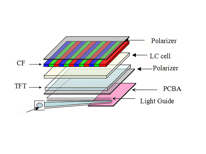
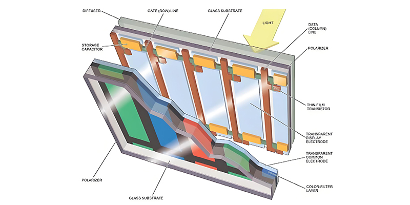
The foundation of any TFT LCD is its array structure, a complex grid of thin-film transistors and pixel electrodes that form the active matrix. This array serves as the backbone for controlling individual pixels, enabling the precise voltage regulation necessary for high-quality image reproduction. Proper array design is critical not only for display performance but also for minimizing issues like lcd screen stains that can occur due to uneven voltage distribution.Lcd screen display.
TFT array fabrication begins with a glass substrate, typically made of soda-lime or aluminosilicate glass, chosen for its flatness, transparency, and thermal stability. The manufacturing process involves several photolithographic steps to create the intricate patterns of electrodes, semiconductors, and insulators that form the transistor matrix.
Each pixel in the array consists of three subpixels (red, green, and blue) in color displays, each controlled by its own TFT. The TFT acts as a switch, controlling the voltage applied to the pixel electrode relative to a common electrode. This voltage determines the orientation of liquid crystal molecules, which in turn modulates the light passing through the pixel.
Critical parameters in TFT array design include pixel pitch (the distance between adjacent pixels), aperture ratio (the percentage of the pixel area that transmits light), and transistor performance characteristics such as on-resistance and off-leakage current. These parameters directly influence display resolution, brightness, contrast ratio, and power consumption.
Modern TFT arrays use amorphous silicon (a-Si), low-temperature polysilicon (LTPS), or indium gallium zinc oxide (IGZO) semiconductors. Each material offers distinct advantages: a-Si is cost-effective for large-area displays, LTPS provides higher electron mobility enabling smaller transistors and higher resolution, while IGZO offers low leakage current and high transparency, beneficial for power efficiency and reducing lcd screen stains caused by current leakage.
The array design must also incorporate storage capacitors, which maintain the pixel voltage during the horizontal blanking interval when the TFT is turned off. The size and placement of these capacitors are carefully engineered to prevent voltage decay that would cause flicker or image distortion, which in severe cases can manifest as lcd screen stains.
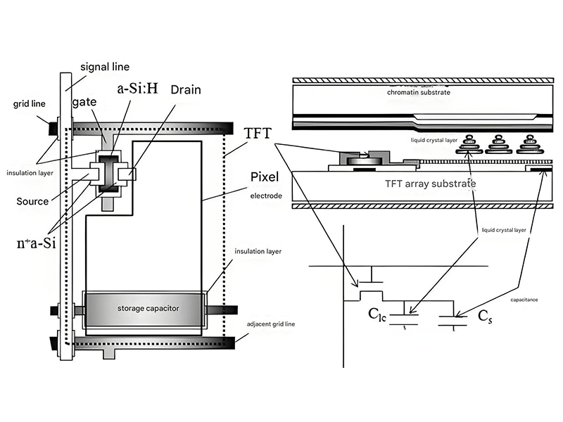
TFT Array Architecture
Cross-sectional view of a typical TFT LCD array showing the glass substrate, gate and source electrodes, semiconductor layer, and pixel structure. Proper design minimizes electron leakage that can cause lcd screen stains.
Key Design Considerations:
- Uniform pixel characteristics across display area
- Minimization of parasitic capacitance
- Optimized aperture ratio for brightness
- Prevention of current leakage causing lcd screen stains
- Thermal management for stable operation
Advanced TFT Array Design Parameters
Transistor Characteristics
The TFT's electrical properties are fundamental to array performance. On/off current ratio, threshold voltage, and field-effect mobility directly impact switching speed and pixel stability. A high on/off ratio (>10⁶) ensures minimal leakage current that could cause image retention or lcd screen stains.
Threshold voltage uniformity across the array is critical, as variations can lead to brightness inconsistencies. Modern fabrication processes achieve threshold voltage variations of less than ±0.5V, significantly reducing the risk of visible lcd screen stains.
Pixel Layout Optimization
Pixel layout design balances multiple competing requirements. The aperture ratio must be maximized for brightness while accommodating the TFT, storage capacitor, and interconnections. In-plane switching (IPS) and vertical alignment (VA) technologies each require distinct pixel architectures.
Color filter design, including material selection and patterning precision, affects color gamut and uniformity. Advanced designs incorporate compensation films to reduce viewing angle dependence and minimize color shifts that might be mistaken for lcd screen stains.
2. Active Matrix TFT LCD Driving Method
The active matrix driving method distinguishes TFT LCDs from their passive matrix predecessors, enabling higher resolution, faster response times, and superior image quality—a benefit that remains prominent even in common comparisons like ips screen vs lcd. This approach uses the TFT at each pixel to actively maintain the pixel voltage during the display's refresh cycle, preventing crosstalk between pixels and reducing issues like LCD screen stains caused by voltage fluctuations.
In active matrix driving, the display operates in a line-scanning mode. The driver electronics sequentially address each row (gate line) by applying a voltage that turns on all TFTs in that row. Simultaneously, data voltages corresponding to the desired pixel brightness are applied to the column (source) lines, charging each pixel's storage capacitor through its conducting TFT.
Once a row has been addressed, the gate voltage is removed, turning off all TFTs in that row. The storage capacitor maintains the pixel voltage until the row is addressed again in the next frame, typically 1/60 to 1/120 of a second later. This maintenance of voltage ensures stable pixel states and reduces flicker, which can contribute to eye strain and the perception of lcd screen stains.
The driving method must account for several electrical characteristics, including the RC time constant of the pixel circuit (resistance of the TFT and capacitance of the pixel and associated wiring). This time constant determines how quickly the pixel charges to the desired voltage, affecting the maximum achievable frame rate.
Voltage levels are carefully calibrated based on the liquid crystal material's properties, typically ranging from 0 to 10 volts. The relationship between applied voltage and light transmission (gamma curve) is non-linear, requiring gamma correction in the driving electronics to ensure accurate brightness reproduction and prevent luminance variations that could appear as lcd screen stains.
Advanced active matrix driving techniques include overdrive, where the data voltage is temporarily increased to speed up liquid crystal response, and local dimming, which adjusts backlight intensity in different regions to improve contrast ratio. These techniques not only enhance performance but also help mitigate potential issues like残影 (image retention) that can lead to permanent lcd screen stains if not properly managed.
Active Matrix Driving Architecture
Block diagram illustrating the interaction between gate drivers, source drivers, and the TFT array. The sequential addressing method minimizes crosstalk and helps prevent lcd screen stains.
Driving Sequence:
- Gate driver activates a single row, turning on all TFTs in that row
- Source drivers apply appropriate voltages to column lines
- Pixel capacitors charge through conducting TFTs
- Gate driver deactivates the row, turning off TFTs
- Capacitors maintain voltage until next refresh cycle
- Process repeats for subsequent rows
Active Matrix Driver Electronics
Gate Drivers
These integrated circuits generate the high-voltage signals required to turn TFTs on and off. Modern gate drivers use level-shifting circuits to convert low-voltage control signals to the 10-30V required by the gate electrodes. They must provide precise timing to prevent row crosstalk that could cause lcd screen stains.
Source Drivers
These ICs convert digital image data into analog voltages applied to the column lines. They incorporate digital-to-analog converters (DACs) with up to 10-bit resolution for precise grayscale control. Advanced source drivers include gamma correction circuitry to ensure consistent brightness across the display and minimize lcd screen stains.
Timing Controller
This critical component synchronizes the operation of gate and source drivers, ensuring proper timing of row addressing and data latching. It receives video data from the host system, performs necessary image processing (scaling, color space conversion), and generates control signals. It also implements compensation algorithms to prevent lcd screen stains.
3. Active Matrix TFT LCD Driving Method Examples
Various implementations of active matrix driving techniques have been developed to address specific application requirements, from mobile devices and lcd screen computer cases to large-format displays. Each approach offers unique advantages in terms of power consumption, response time, and image quality, with specific mechanisms to prevent lcd screen stains.
1. Voltage-Controlled Active Matrix Driving
This most common implementation uses voltage-mode source drivers that apply precise voltages to each pixel based on the desired transmittance. The driver ICs contain DACs that convert digital grayscale values to analog voltages, typically in the range of 0-5V for mobile displays and 0-10V for larger panels.
A key feature is the use of alternating current (AC) driving, where the polarity of the voltage applied to the pixel is reversed with each frame. This alternating polarity prevents electrochemical degradation of the liquid crystal material and electrode surfaces, which could lead to permanent lcd screen stains and reduced display lifespan.
2. Current-Programmed Driving
Current-programmed driving methods, used primarily in high-brightness applications, control the current through the liquid crystal rather than the voltage. This approach offers improved grayscale linearity and temperature stability, as current is less affected by temperature-induced changes in liquid crystal properties.
In this method, each source driver outputs a specific current that charges the pixel capacitor to the voltage required to maintain that current. The technique is particularly effective for preventing luminance variations across temperature gradients, which can appear as lcd screen stains in extreme operating conditions.
3. Dual-Gate Driving
Dual-gate TFT configurations use two independent gates per transistor, allowing more precise control over the on/off state. This advanced technique reduces leakage current significantly, enabling longer frame hold times and lower power consumption – particularly beneficial for mobile devices.
The reduced leakage helps maintain stable pixel voltages over extended periods, minimizing image retention that could lead to lcd screen stains. This makes dual-gate driving ideal for applications where static images are displayed for long durations, such as digital signage and instrument panels.
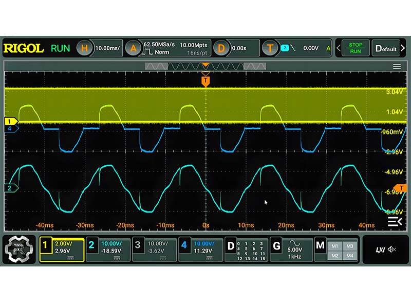
AC Driving Waveforms
Voltage waveforms demonstrating alternating polarity driving, a critical technique for preventing electrochemical degradation and lcd screen stains in active matrix displays.
Comparative Analysis of Driving Methods
| Driving Method | Power Efficiency | Response Time | Resistance to Stains | Cost |
|---|---|---|---|---|
| Voltage-Controlled | Good | Excellent | Good | Low |
| Current-Programmed | Fair | Good | Excellent | Medium |
| Dual-Gate | Excellent | Good | Excellent | High |
Dual-Gate TFT Structure
Cross-sectional view of a dual-gate TFT showing the separate control and drive gates, which provide enhanced leakage current control to prevent lcd screen stains.
Application-Specific Active Matrix Driving Implementations
Mobile Display Driving
Mobile TFT LCDs employ low-voltage driving (typically 3.3V) to minimize power consumption. They often use adaptive refresh rates, reducing from 60Hz to 30Hz or lower when displaying static content. This not only saves battery life but also reduces the potential for lcd screen stains by minimizing pixel voltage changes during static image display.
In-cell touch integration combines the touch sensor with the display matrix, requiring specialized driving techniques to separate display and touch signals. This integration demands precise timing control to prevent interference that could manifest as noise or lcd screen stains.
Large-Format Display Driving
Large LCD panels (32" and above) use tiled driver architectures, with multiple gate and source driver ICs distributed along the panel edges. This approach reduces signal propagation delays and minimizes voltage drops across long interconnections, which could cause brightness variations resembling lcd screen stains.
Many large displays implement local dimming, where the backlight is divided into zones controlled independently based on image content. The LCD driving must be coordinated with backlight levels to maximize contrast ratio while preventing blooming artifacts that might be mistaken for lcd screen stains.
4. Passive Matrix Driving Method
While active matrix technology dominates modern LCD applications, passive matrix driving remains relevant for specific low-cost, low-power applications. Unlike active matrix displays, passive matrix LCDs lack transistors at each pixel, instead using a simple grid of row and column electrodes to address pixels—an attribute that makes them well-suited for mini lcd screen (where space and power constraints prioritize simplicity over high performance). This fundamental difference results in distinct performance characteristics and different approaches to preventing issues like lcd screen stains.
In passive matrix driving, also known as simple matrix driving, pixels are addressed by applying voltage between selected row and column electrodes. When a voltage exceeding the liquid crystal threshold is applied across a pixel, it switches state. This process is repeated sequentially for each row, with appropriate column voltages applied to create the desired image pattern.
A significant limitation of passive matrix technology is crosstalk, where unaddressed pixels receive voltage due to the voltage division across the matrix. This effect increases with display size and resolution, making passive matrix impractical for large, high-resolution displays. Crosstalk can manifest as unintended brightness variations that appear similar to lcd screen stains, though they have a different root cause.
To mitigate crosstalk, passive matrix displays use a multiplexing factor (the ratio of rows to active time per row) that limits their maximum size and resolution. The duty cycle (percentage of time a pixel is addressed per frame) decreases as the number of rows increases, reducing brightness and contrast ratio.
Passive matrix driving employs several techniques to improve performance, including bias voltage application to unselected rows and columns. By applying a fraction of the threshold voltage to unselected lines, the effective voltage across unaddressed pixels is reduced below the switching threshold, minimizing crosstalk and associated artifacts that might be mistaken for lcd screen stains.
Response time in passive matrix displays is typically slower than in active matrix designs, as there's no storage capacitor to maintain the pixel state between refreshes. This makes them unsuitable for fast-moving content but adequate for static or slow-changing information displays.
Despite their limitations, passive matrix LCDs offer advantages in cost, power consumption, and simplicity, making them suitable for applications like digital watches, calculators, simple industrial displays, and low-cost consumer electronics. Their reduced complexity also means they are less prone to certain types of lcd screen stains related to transistor degradation, though they remain susceptible to image retention under static display conditions.
Passive Matrix Architecture
Simplified structure of a passive matrix LCD showing the row and column electrode grid. Without TFTs, voltage control is less precise, requiring specialized techniques to prevent artifacts resembling lcd screen stains.
Key Characteristics:
- No active components (transistors) at pixel level
- Sequential row addressing with column data
- Limited resolution and size due to crosstalk
- Lower power consumption than active matrix
- Susceptible to certain types of lcd screen stains
Bias Voltage Technique
To reduce crosstalk, passive matrix displays apply a bias voltage (Vb) to unselected rows:
This reduces the voltage across unaddressed pixels, minimizing unwanted activation that could appear as lcd screen stains.
Active Matrix vs. Passive Matrix Driving: Comprehensive Comparison
| Characteristic | Active Matrix TFT LCD | Passive Matrix LCD |
|---|---|---|
| Pixel Structure | Contains TFT and storage capacitor at each pixel | Simple intersection of row and column electrodes |
| Resolution Capability | High (4K, 8K, and beyond) | Limited (typically QVGA or lower) |
| Response Time | Fast (1-10ms) | Slow (50-200ms) |
| Viewing Angle | Wide (especially with IPS technology) | Narrow |
| Power Consumption | Moderate to high | Low |
| Cost | Higher (complex fabrication) | Lower (simpler structure) |
| Susceptibility to LCD Screen Stains | Moderate (controlled by TFT design) | Higher (due to voltage crosstalk) |
| Typical Applications | Smartphones, monitors, TVs, tablets | Calculators, watches, simple displays |
Mitigation of LCD Screen Stains in Passive Matrix Displays
While passive matrix displays are generally more prone to certain artifacts resembling lcd screen stains, several techniques help mitigate these issues:
- Optimized bias voltage selection to minimize crosstalk-induced brightness variations
- Frame inversion techniques to prevent DC voltage components that cause material degradation
- Refresh rate optimization to balance power consumption and image stability
- Specialized liquid crystal materials with reduced memory effects
- Software-based image shifting for static content to prevent permanent lcd screen stains
Conclusion
The design and driving of liquid crystal displays represent a sophisticated integration of materials science, electrical engineering, and precision manufacturing. From the complex TFT arrays that form the backbone of active matrix displays to the simpler electrode grids of passive matrix designs, each approach offers distinct advantages for specific applications.
A thorough understanding of these technologies is essential for optimizing display performance, extending lifespan, and preventing common issues like lcd screen stains. As display technology continues to evolve, with increasing resolution, faster response times, and lower power consumption, the principles outlined in this guide remain fundamental to LCD engineering.
Whether implementing advanced active matrix driving techniques for high-performance displays or optimizing passive matrix designs for cost-sensitive applications, the core challenges of voltage control, crosstalk minimization, and prevention of lcd screen stains remain central to successful LCD implementation.