Thin Film Transistor (TFT) technology forms the backbone of modern lcd screen display systems, enabling the high-resolution, fast-response displays we rely on in smartphones, televisions, monitors, and industrial equipment. The array design process represents the critical foundation of TFT manufacturing, where precision engineering meets cutting-edge materials science to create the complex structures that control each pixel.
This comprehensive guide explores the five essential engineering disciplines that define world-class TFT array development. From initial system architecture to final inspection protocols, each phase contributes to the performance, efficiency, and reliability of the final lcd screen display. Our engineering approach integrates advanced simulation, material science, and manufacturing expertise to push the boundaries of what's possible in display technology.
The foundation of any successful TFT lcd screen display begins with comprehensive system design engineering diagrams—critical for developing a custom lcd screen—that translate functional requirements into technical specifications. These diagrams serve as the blueprint for the entire development process, integrating mechanical, electrical, and optical considerations to meet the unique needs of custom displays.
Our system design process starts with requirements analysis, where we define resolution, refresh rate, power consumption, and environmental operating parameters. This information feeds into block diagrams that map out the major subsystems: pixel array, driver circuitry, backlighting, and control interfaces. Each block undergoes detailed specification to ensure compatibility and performance targets.
Critical to this phase is the development of interface diagrams that define signal protocols between the TFT array and external components. Timing diagrams ensure synchronization between row and column drivers, preventing crosstalk and ensuring stable lcd screen display performance. Thermal management diagrams address heat dissipation pathways, crucial for maintaining performance in high-brightness applications.
Our system design engineers utilize advanced simulation tools to validate designs before prototyping, analyzing factors such as power distribution, signal integrity, and optical performance. This virtual validation reduces development cycles and ensures that the final lcd screen display meets all performance criteria.
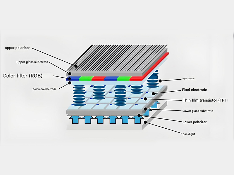
Figure 1: System architecture diagram showing the integration of key components in a TFT LCD display system
Key Elements of System Design Engineering Diagrams
- Functional block diagrams defining subsystem interfaces and interactions
- Signal flow diagrams detailing data and control pathways throughout the lcd screen display
- Power distribution schematics ensuring stable voltage delivery to all components
- Mechanical integration diagrams showing layer stackups and dimensional constraints
- Thermal management layouts optimizing heat dissipation for reliable operation
- Optical path diagrams modeling light propagation and polarization effects
Array design engineering represents the core of TFT lcd screen display technology, where millions of tiny transistors are arranged in a precise grid to control individual pixels. This complex architecture requires meticulous engineering to balance performance, power efficiency, and manufacturing feasibility— a balance that becomes even more critical for emerging products like flexible lcd screen, which demand array designs that are both lightweight and resilient to repeated bending without pixel or transistor failure.
TFT Structure Design
Our engineers optimize thin film transistor structures, selecting materials and geometries that balance electron mobility, on/off ratio, and threshold voltage stability for superior lcd screen display performance.
Pixel Architecture
Pixel design focuses on maximizing aperture ratio while minimizing crosstalk between adjacent pixels, ensuring bright, uniform lcd screen display performance with accurate color reproduction.
Interconnect Layout
Metal line routing is optimized for minimal resistance and capacitance, reducing signal delay and ensuring fast response times crucial for high-performance lcd screen display applications.
Figure 2: Cross-sectional view of TFT array structure showing layered architecture
The array design process begins with defining the pixel pitch and resolution, which directly influence the lcd screen display quality. Our engineers perform detailed simulations to determine the optimal TFT size and placement within each pixel, maximizing light transmission while ensuring reliable switching.
Material selection plays a critical role in array performance. We evaluate various semiconductor materials, including amorphous silicon (a-Si), low-temperature poly-silicon (LTPS), and indium gallium zinc oxide (IGZO), selecting the optimal material based on the lcd screen display application requirements. Each material offers distinct advantages in terms of electron mobility, manufacturing temperature, and cost.
Array design must also account for manufacturing processes, with our engineers working closely with fabrication teams to develop layouts that minimize defects and maximize yield. This includes designing redundancy into critical lines and implementing test structures that allow for in-process monitoring of array performance.
For high-resolution lcd screen display applications, our engineers employ advanced techniques such as multi-domain vertical alignment (MVA) and in-plane switching (IPS) to improve viewing angles and color consistency. These technologies require sophisticated array designs that precisely control liquid crystal orientation across the display surface.
Array Design Performance Metrics
Chart 1: Performance comparison of different array designs across key metrics
Driver circuit design represents the critical interface between the control system and the TFT array, translating digital signals into the precise voltage levels required to activate each pixel— a role that becomes more complex for lcd touch screen, where circuits must synchronize display signal output with touch input detection to avoid latency. The efficiency and performance of these circuits directly impact the lcd screen display quality, power consumption, and response time (including touch response speed for touch-enabled models).
Row and Column Driver Architecture
TFT lcd screen display systems utilize a matrix addressing scheme where row drivers (gate drivers) select individual rows while column drivers (source drivers) provide the appropriate voltage to each column. Our driver circuit designs optimize this architecture to minimize power consumption while maximizing switching speed.
Gate driver circuits must deliver sufficient voltage to turn on TFTs across the entire row, accounting for voltage drops that occur over long distances. We implement advanced level-shifting circuits that convert low-voltage control signals to the higher voltages required for reliable TFT operation.
Source driver circuits require high-precision digital-to-analog converters (DACs) to generate the precise voltage levels needed for accurate grayscale reproduction in the lcd screen display. Our designs incorporate calibration mechanisms to compensate for component variations and ensure uniform output across all channels.
For large-format displays, we implement distributed driver architectures that reduce signal propagation delays and minimize electromagnetic interference (EMI). This modular approach also simplifies scaling to different lcd screen display sizes and resolutions.
Figure 3: Driver circuit architecture showing integration with TFT array
Advanced Driving Methods
- Frame Rate Control (FRC): Enhances grayscale resolution by rapidly switching between adjacent gray levels
- Overdrive Technology: Accelerates pixel response by applying higher voltages during transitions
- Local Dimming: Controls backlight intensity in zones to improve contrast ratio
- Adaptive Refresh Rate: Adjusts frame rate based on content to reduce power consumption
Driving Method Comparison
| Driving Method | Power Efficiency | Response Time | Complexity | Best For |
|---|---|---|---|---|
| Static Driving | Low | Fast | High | Small lcd screen display panels |
| Time-Division Driving | Medium | Medium | Medium | Medium-sized displays |
| Active Matrix Driving | High | Very Fast | Very High | High-resolution lcd screen display panels |
| Dual-Gate Driving | High | Ultra Fast | Extremely High | Premium gaming displays |
Our driver circuit designs incorporate adaptive voltage scaling that adjusts operating voltages based on lcd screen display content and temperature, significantly reducing power consumption without compromising performance. For mobile applications, we've developed ultra-low-power standby modes that maintain display state with minimal current draw.
Array pattern design engineering is particularly critical for specialized displays like the lcd screen for pc case—these screens, tailored to fit computer chassis and show hardware metrics, rely on precise photomask patterns to balance compact size with clear display. This phase transforms circuit concepts into such patterns, bridging design and manufacturing to ensure that the lcd screen display (including pc case variants) can be produced efficiently while meeting all performance specifications.
Pattern design begins with layout synthesis, where our engineers convert schematic designs into geometric patterns using advanced EDA (Electronic Design Automation) tools. These patterns define the shape and placement of all conductive, semiconductor, and insulating layers in the TFT array.
For high-resolution lcd screen display panels, pattern designers must work with feature sizes approaching the limits of photolithography. Our engineers utilize resolution enhancement techniques (RET) such as optical proximity correction (OPC) and phase-shift masks to ensure that tiny features are reproduced accurately during manufacturing.
Pattern design must account for the entire fabrication process flow, including etch bias, deposition effects, and planarization. Our 3D process simulations predict how patterns will transform through each manufacturing step, allowing designers to compensate for process-induced distortions in the original pattern layout.
The layout of test structures is integrated into the array pattern design, providing in-line monitoring of critical parameters during manufacturing. These test structures measure TFT performance, line resistance, and insulation properties, enabling process control and ensuring consistent lcd screen display quality.
Our pattern design engineers collaborate closely with yield enhancement teams to identify and eliminate layout-related failure modes. This includes optimizing pattern density to prevent thin-film stress issues, designing robust interconnects, and implementing redundancy for critical paths in the lcd screen display architecture.
Figure 4: Array pattern design details showing TFT and pixel layouts
Pattern Design Considerations
- Photolithography resolution limits
- Etch and deposition process effects
- Overlay alignment tolerances
- Electrical performance optimization
- Manufacturing yield improvement
- Thermal stress minimization
Pattern Design Verification Process
Design Rule Check
Verification that all patterns comply with manufacturing constraints and minimum feature sizes
Electrical Rule Check
Validation of electrical performance including resistance, capacitance, and signal integrity
Process Simulation
Modeling of pattern transformation through manufacturing steps to predict final geometry
Visual Inspection
Manual review of critical areas to ensure pattern integrity and manufacturability
Inspection design engineering ensures that every lcd screen display meets stringent quality standards through the development of comprehensive testing protocols and inspection systems—systems centered on the lcd screen tester (a specialized device that performs pixel defect scans, brightness uniformity checks, and color accuracy verifications). This discipline combines advanced imaging technology, data analysis, and automated defect classification (integrated into the LCD screen tester) to identify and characterize imperfections at every stage of manufacturing.
Figure 5: Automated optical inspection system for TFT array quality control
Key Inspection Stages
- Film deposition quality verification
- Pattern transfer accuracy inspection
- TFT electrical performance testing
- Array interconnect continuity checking
- Pixel functionality validation
- Final lcd screen display performance evaluation
Inspection System Design
Our inspection design engineers develop custom systems tailored to the specific requirements of each lcd screen display product. These systems combine high-resolution cameras, precision motion control, and specialized lighting to detect defects that would impact performance or reliability.
For array inspection, we utilize multiple imaging modalities including bright-field, dark-field, and phase-contrast microscopy to identify different types of defects. Advanced image processing algorithms enhance defect visibility and enable automated detection, even in the most complex lcd screen display patterns.
Electrical inspection systems incorporate probe cards or non-contact testing methods to verify TFT performance parameters across the entire array. These systems can measure threshold voltage, on-current, off-current, and leakage with high precision, ensuring uniform performance across the lcd screen display.
Our inspection data management systems aggregate results from all inspection stages, providing process engineers with actionable insights to identify and correct manufacturing issues. Statistical process control (SPC) algorithms detect trends in defect occurrence, enabling proactive process adjustments before yield is impacted.
Defect Classification and Analysis
Effective inspection requires robust defect classification systems that can distinguish between critical and non-critical imperfections in the lcd screen display array. Our engineers have developed sophisticated machine learning algorithms that can identify and categorize thousands of defect types with high accuracy.
Common Defect Types
- Particle contamination and foreign materials
- Pattern defects including missing or extra material
- Electrical defects such as short circuits or open circuits
- Film defects including pinholes and thickness variations
- TFT performance outliers affecting lcd screen display uniformity
Inspection Data Utilization
- Yield improvement through root cause analysis
- Process control and equipment performance monitoring
- Quality trend analysis and predictive maintenance
- Customer-specific quality requirement verification
- Continuous improvement of lcd screen display manufacturing processes
Advancing TFT LCD Array Design Excellence
The five engineering disciplines detailed here represent the foundation of world-class TFT lcd screen display development. By integrating system design, array engineering, driver circuit design, pattern layout, and inspection methodologies, we create display solutions that push the boundaries of performance, efficiency, and reliability.
Our commitment to engineering excellence ensures that every lcd screen display meets the most demanding application requirements, from ultra-high-resolution monitors to ruggedized industrial displays. Through continuous innovation in each of these critical areas, we deliver display technologies that enable the next generation of visual experiences.