1. Latest Technological Trends in LCDs
The liquid crystal display (LCD) industry continues to evolve at a rapid pace, driven by consumer demand for higher quality displays in smartphones, televisions, monitors, and automotive applications. One of the most significant trends is the integration of advanced backlighting technologies, particularly mini-LED and micro-LED solutions, which offer superior contrast ratios and more precise local dimming compared to traditional LED backlighting. These technologies enable displays to achieve deeper blacks and more vibrant colors, approaching the quality of OLED panels while maintaining the cost advantages of LCD technology.
Another key trend is the development of higher resolution displays, with 8K resolution becoming increasingly common in large-format televisions. This advancement not only enhances visual clarity but also enables more immersive viewing experiences, especially when combined with high dynamic range (HDR) technology. The implementation of these high-resolution displays has been greatly supported by advancements in cpu lcd screen animations processing capabilities, allowing for smooth rendering of complex visual content.
In addition to resolution improvements, there is a growing focus on energy efficiency. Manufacturers are developing LCD panels that consume less power while maintaining brightness levels, making them ideal for battery-powered devices such as laptops and tablets. This is achieved through the use of more efficient liquid crystal materials, improved backlighting systems, and advanced power management technologies.
The integration of touch functionality into LCD panels is another trend gaining momentum, particularly in automotive and industrial applications. In-cell touch technologies, where touch sensors are integrated directly into the LCD panel rather than as a separate layer, are becoming more prevalent due to their thinner profile and improved light transmission. This technology also enhances the responsiveness of cpu lcd screen animations, providing a more seamless user experience.
Finally, the emergence of flexible LCD displays represents a significant technological breakthrough. While OLED technology has dominated the flexible display market, recent advancements in LCD technology have enabled the production of bendable and rollable LCD panels. These displays maintain the cost advantages of LCDs while offering new form factors and applications, from foldable smartphones to rollable televisions. The development of flexible LCDs has required innovations in both materials science and manufacturing processes, paving the way for new product categories and user experiences.
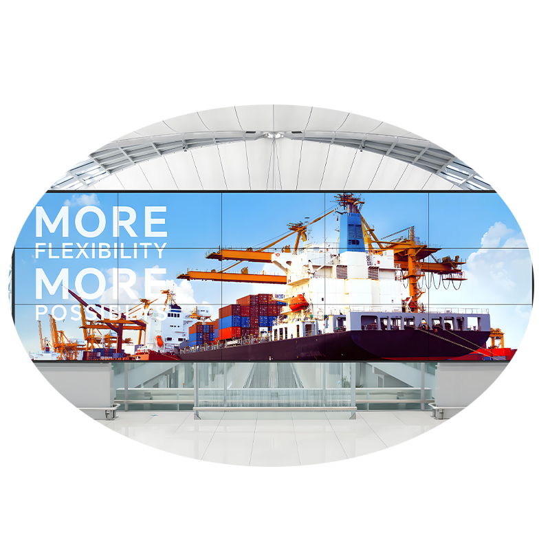
Growth Projection of LCD Technologies
Market share distribution and growth projections for various LCD technologies, highlighting the increasing adoption of advanced solutions.
2. Improving TFT LCD Aperture Ratio
The aperture ratio of a TFT LCD refers to the percentage of the pixel area that is actually used for light transmission, as opposed to the area occupied by the thin-film transistors and wiring. A higher aperture ratio directly translates to a brighter display with better contrast, as more light can pass through each pixel. This is particularly important for mobile devices used outdoors and for reducing power consumption, as a higher aperture ratio allows for equivalent brightness with less backlight power.
One of the primary methods for improving aperture ratio is the development of more compact TFT structures. Traditional amorphous silicon (a-Si) TFTs have relatively large footprints, limiting the aperture ratio. The transition to low-temperature polysilicon (LTPS) TFTs has enabled significant reductions in transistor size, allowing for a larger light-transmitting area within each pixel. LTPS technology also offers higher electron mobility, which improves display performance in applications requiring complex cpu lcd screen animations.
Advanced pixel design techniques have also contributed to aperture ratio improvements. These include the development of new pixel layouts that minimize the area occupied by wiring and transistors while maintaining structural integrity. For example, some manufacturers have adopted a staggered pixel arrangement or reduced the number of wires by sharing components between adjacent pixels. These innovations not only increase the aperture ratio but also improve the uniformity of the display, reducing visible pixel structures.
Another approach is the implementation of transparent conductive materials for the pixel electrodes and wiring. Indium tin oxide (ITO) has long been the standard material, but new alternatives such as indium zinc oxide (IZO) and graphene-based materials offer better conductivity and transparency. These materials allow for narrower wiring, reducing the area they occupy while maintaining signal integrity. This is particularly beneficial for high-resolution displays, where pixel density is high and space is at a premium.
The development of three-dimensional (3D) TFT structures represents a more radical approach to improving aperture ratio. By stacking transistor components vertically rather than placing them side by side in the same plane, manufacturers can significantly reduce the footprint of each pixel's active components. This technology is still in its early stages but shows great promise for future high-performance displays. When combined with advanced driving technologies, these high-aperture ratio displays can deliver exceptional brightness and contrast while supporting the complex visual requirements of modern cpu lcd screen animations.
Aperture Ratio Improvement Techniques
LTPS TFT Integration
30-40% reduction in transistor footprint compared to a-Si TFTs
Advanced Pixel Design
Optimized layouts increasing effective area by 15-25%
Transparent Conductors
50% narrower wiring with improved conductivity
3D TFT Structures
Potential for 50%+ aperture ratio improvement in next generation
3. Wide Viewing Angle Technology
One of the historical limitations of LCD technology has been its narrow viewing angle compared to cathode ray tube (CRT) displays. Early LCDs suffered from significant color shifts and contrast reduction when viewed from off-center angles, making them less suitable for applications where multiple viewers might be watching simultaneously, such as in home theaters or conference rooms. Over the past decade, however, significant advancements in wide viewing angle technologies have largely overcome this limitation.
The most widely adopted solution for improving viewing angles in TFT LCDs is the in-plane switching (IPS) technology. Unlike traditional twisted nematic (TN) LCDs, where liquid crystals twist to control light passage, IPS displays align their liquid crystals parallel to the panel surface. When voltage is applied, the crystals rotate in the same plane rather than twisting, which allows for more consistent light transmission across a wider range of viewing angles. This technology not only improves viewing angles but also enhances color accuracy and reduces response time, making it ideal for applications requiring precise color reproduction and smooth cpu lcd screen animations.
Another important wide viewing angle technology is vertical alignment (VA) LCDs. VA panels align their liquid crystals perpendicular to the substrate when no voltage is applied, resulting in very high contrast ratios. When voltage is applied, the crystals tilt to control light transmission. Modern multi-domain vertical alignment (MVA) and patterned vertical alignment (PVA) technologies divide each pixel into multiple sub-pixels with different alignment directions, significantly improving viewing angles while maintaining the high contrast characteristics of VA panels. This makes VA technology particularly popular in large-screen televisions where both contrast and viewing angle are important.
Advanced compensation films have also played a crucial role in improving viewing angles. These optical films are designed to counteract the phase shifts that occur when light passes through liquid crystals at oblique angles, reducing color distortion and maintaining contrast. Compensation films are often used in conjunction with IPS or VA technologies to further enhance viewing angle performance. The development of these films has been critical for enabling the thin, lightweight form factors of modern LCD displays while maintaining wide viewing angles.
Recent innovations in liquid crystal materials have further expanded viewing angles. New chiral smectic and blue phase liquid crystals offer faster response times and wider viewing angles compared to traditional nematic liquid crystals. These advanced materials are particularly promising for next-generation displays requiring both high performance and energy efficiency. When combined with advanced driving algorithms, these materials can deliver exceptional viewing angle performance while supporting the demanding visual requirements of modern applications, including high-resolution cpu lcd screen animations and interactive content.
Viewing Angle Comparison
IPS vs VA vs TN technologies at various viewing angles
IPS Technology
178°
Horizontal/Vertical
VA Technology
178°
Horizontal/Vertical
TN Technology
140°/120°
Horizontal/Vertical
4. Improving Response Time
Response time is a critical performance metric for TFT LCDs, referring to the time it takes for a pixel to change from one state to another, typically measured in milliseconds (ms). Slow response times can result in motion blur, ghosting, and trailing artifacts, particularly in fast-moving content such as video games, sports broadcasts, and action movies. Over the years, significant advancements have been made in reducing LCD response times, making them competitive with other display technologies for even the most demanding applications.
One of the primary methods for improving response time is the development of advanced liquid crystal materials. Traditional nematic liquid crystals have relatively slow response times, but new formulations with lower viscosity and higher elastic constants allow for faster switching. These advanced materials can reduce response times by 30-50% compared to older formulations, enabling smoother motion in fast-paced content. This is particularly important for supporting the high frame rates required for realistic cpu lcd screen animations and interactive applications.
Advanced driving techniques have also played a crucial role in reducing response times. Overdrive technology, where a higher voltage is applied to pixels during transitions to speed up the liquid crystal movement, has become standard in modern LCDs. The latest implementations use adaptive overdrive algorithms that adjust the voltage based on the specific transition (e.g., from dark to light or light to dark) and even the content being displayed. This adaptive approach minimizes overshoot artifacts while maximizing speed, resulting in response times as low as 1-2 ms for some transitions.
The adoption of higher refresh rates has further improved the perceived motion clarity of LCD displays. While traditional displays operate at 60Hz (60 frames per second), modern gaming monitors and high-performance televisions often feature 120Hz, 144Hz, or even 240Hz refresh rates. When combined with fast response times, these higher refresh rates significantly reduce motion blur and improve the smoothness of fast-moving content. This is particularly beneficial for competitive gaming, where split-second reactions are crucial, and for high-quality cpu lcd screen animations that require fluid motion.
The development of new pixel structures and electrode designs has also contributed to faster response times. For example, some manufacturers have implemented dual-domain or multi-domain pixel structures that allow for more uniform and faster liquid crystal rotation. Additionally, the use of advanced TFT technologies such as LTPS and oxide semiconductors has enabled faster switching speeds and more precise control over individual pixels. These innovations, combined with improvements in backlighting technologies like strobing (where the backlight flashes in sync with frame updates), have pushed LCD response times to levels that were unimaginable just a decade ago, making them suitable for even the most demanding visual applications.
Response Time Improvement Methods
Current Achievable Response Times
Enabling smooth motion in gaming and cpu lcd screen animations
5. Current Status of LCD TV Development
LCD technology continues to dominate the television market, offering a compelling balance of performance, size, and affordability. The current generation of LCD TVs incorporates numerous advancements that have significantly narrowed the performance gap with OLED technology, particularly in the areas of contrast ratio, color accuracy, and motion handling. One of the most notable developments is the widespread adoption of mini-LED backlighting, which has revolutionized LCD TV performance.
Mini-LED backlighting uses thousands of tiny LEDs arranged in a grid behind the LCD panel, enabling much more precise local dimming than traditional LED backlighting. This results in significantly improved contrast ratios, with deeper blacks and brighter highlights, approaching the performance of OLED displays. Mini-LED TVs also offer better uniformity and reduced blooming around bright objects on dark backgrounds. This technology has been particularly well-received in larger screen sizes, where it provides an optimal balance between performance and cost. The improved brightness and contrast of mini-LED TVs also enhance the viewing experience for cpu lcd screen animations and HDR content.
Resolution continues to be a key area of development, with 4K resolution now standard across most mid-to-high-end LCD TVs, and 8K resolution gaining traction in larger screen sizes. While 8K content remains limited, these TVs employ advanced upscaling technologies that improve the quality of lower-resolution content. Additionally, the higher pixel density of 8K displays enhances the viewing experience for larger screens, where individual pixels might be visible with lower resolutions at typical viewing distances.
Smart TV functionality has become increasingly sophisticated, with modern LCD TVs featuring powerful processors that handle not only video processing but also a wide range of connected features. These include built-in streaming services, voice control, home automation integration, and even gaming capabilities. The latest LCD TVs often include dedicated gaming features such as variable refresh rate (VRR), auto low latency mode (ALLM), and high frame rate support, making them popular choices for gaming enthusiasts. These features, combined with improved response times, make modern LCD TVs excellent platforms for gaming and interactive cpu lcd screen animations.
Energy efficiency has also been a major focus, with recent LCD TVs consuming significantly less power than their predecessors while maintaining or improving brightness levels. This has been achieved through a combination of more efficient backlighting systems, improved panel technology, and advanced power management features. Additionally, the trend toward larger screen sizes continues, with 75-inch and 85-inch models becoming increasingly common in the mainstream market, while even larger sizes (98 inches and above) are becoming more accessible.
Looking forward, the LCD TV market is expected to continue evolving with further improvements in mini-LED technology, including even more LEDs for enhanced local dimming, and the potential introduction of micro-LED technology in larger screen sizes. These advancements, combined with ongoing improvements in panel technology, processing power, and smart features, ensure that LCD TVs will remain a dominant force in the television market for the foreseeable future.
Key Features of Modern LCD TVs
Mini-LED Backlighting
1000+ dimming zones for superior contrast
120Hz Refresh
Smooth motion for sports and gaming
Gaming Features
VRR, ALLM, low input lag
Smart Functionality
Advanced processors, voice control
6. Innovations in TFT LCD Manufacturing Technology
The manufacturing process for TFT LCDs has undergone significant innovations over the years, driven by the need to increase production efficiency, reduce costs, and enable new display technologies. These advancements have not only improved the quality and performance of LCD panels but have also made larger, higher-resolution displays more accessible to consumers.
One of the most significant manufacturing innovations is the transition to larger glass substrates. Early LCD production used relatively small substrates, but modern fabs now use Generation 10.5/11 substrates, which measure approximately 3370mm × 2940mm. These larger substrates allow manufacturers to produce more panels per sheet, reducing production costs and enabling the efficient manufacturing of very large displays (65 inches and above). The transition to larger substrates has required significant advancements in handling equipment, deposition technologies, and precision cutting techniques to maintain quality standards.
Advanced deposition techniques have also played a crucial role in improving TFT LCD manufacturing. Atomic layer deposition (ALD) and chemical vapor deposition (CVD) processes have been refined to create thinner, more uniform layers of materials with better electrical properties. These techniques enable the production of smaller, more efficient TFTs, which contribute to higher aperture ratios and improved display performance. Additionally, new sputtering technologies allow for more precise control over the deposition of transparent conductive materials like ITO, resulting in better conductivity and transparency.
The development of maskless lithography techniques represents another important innovation in LCD manufacturing. Traditional photolithography uses expensive masks to pattern each layer of the TFT array, which becomes increasingly challenging with larger substrates and higher resolutions. Maskless lithography, which uses direct laser writing or electron beam techniques, eliminates the need for physical masks, reducing costs and enabling faster prototyping of new display designs. This technology is particularly valuable for producing high-resolution displays with complex pixel structures, which are essential for supporting advanced cpu lcd screen animations and high-definition content.
Roll-to-roll manufacturing is an emerging technology that promises to revolutionize LCD production, particularly for flexible displays. This process involves depositing thin films onto a flexible substrate that is rolled through the manufacturing line, similar to newspaper printing. Roll-to-roll manufacturing offers the potential for continuous, high-speed production at significantly lower costs compared to traditional sheet-based processes. While still in the early stages of adoption for LCDs, this technology could enable the mass production of flexible and even foldable LCD displays in the coming years.
Finally, artificial intelligence and machine learning are being increasingly integrated into LCD manufacturing processes. These technologies are used to optimize production parameters, predict and prevent defects, and improve quality control. By analyzing vast amounts of production data in real-time, AI systems can make minute adjustments to the manufacturing process, resulting in higher yields and more consistent product quality. This not only reduces costs but also enables the production of displays with tighter performance tolerances, which is essential for applications requiring precise color matching and uniform brightness, such as video walls and professional cpu lcd screen animations systems.
Evolution of LCD Substrate Sizes
320×400
550×650
1100×1300
2200×2500
3370×2940
Key Manufacturing Innovations
- Advanced ALD/CVD deposition techniques for thinner, more uniform layers
- Maskless lithography reducing costs and enabling complex designs
- Roll-to-roll manufacturing for flexible displays
- AI-driven process optimization and quality control
- Precision cutting technologies for minimal material waste
7. Low-Temperature Polycrystalline Silicon LCDs
Low-Temperature Polycrystalline Silicon (LTPS) LCD technology represents a significant advancement over traditional amorphous silicon (a-Si) TFT LCDs. LTPS is produced by crystallizing amorphous silicon at temperatures between 300-500°C, significantly lower than the temperatures required for high-temperature polysilicon. This lower processing temperature allows LTPS to be deposited on glass substrates, making it compatible with standard LCD manufacturing processes while offering superior performance characteristics.
One of the primary advantages of LTPS technology is its significantly higher electron mobility compared to a-Si. This allows for smaller TFTs with faster switching speeds, resulting in higher aperture ratios and improved display brightness. The smaller transistor size also enables higher pixel densities, making LTPS displays ideal for high-resolution applications such as smartphones, tablets, and small to medium-sized monitors. The faster switching speeds of LTPS TFTs also contribute to improved response times, enhancing the performance of cpu lcd screen animations and fast-moving content.
LTPS technology also enables the integration of additional functionality directly into the display panel. This includes touch sensors, driver circuits, and even image processing capabilities, which can reduce the overall thickness and complexity of display modules. In-cell touch technology, where the touch sensors are integrated into the LCD panel rather than as a separate layer, is particularly well-suited to LTPS displays. This integration not only reduces thickness but also improves light transmission and touch sensitivity, resulting in brighter displays with more responsive touch interfaces.
Energy efficiency is another key advantage of LTPS LCDs. The higher electron mobility of LTPS TFTs allows them to operate at lower voltages, reducing power consumption compared to a-Si displays. This makes LTPS technology particularly attractive for battery-powered devices such as smartphones and tablets, where power efficiency is critical. Additionally, the improved aperture ratio of LTPS displays means that backlighting can be dimmed while maintaining the same perceived brightness, further reducing power consumption.
In recent years, LTPS technology has been combined with other advanced display technologies to create even more capable displays. For example, LTPS backplanes are often used in OLED displays to provide precise control over each pixel, and they are also integral to flexible display technologies. The combination of LTPS with quantum dot technology has resulted in displays with enhanced color gamuts and improved color accuracy. These advanced LTPS displays are capable of rendering highly realistic cpu lcd screen animations with vibrant colors and smooth motion.
While LTPS technology offers numerous advantages, it does come with higher manufacturing costs compared to a-Si. However, as production volumes have increased and manufacturing processes have matured, these cost differences have narrowed. Today, LTPS technology is widely used in high-end smartphones, tablets, and premium small to medium-sized displays where its performance advantages justify the additional cost. As manufacturing techniques continue to improve, LTPS is expected to find applications in an even wider range of devices, further expanding its market presence.
LTPS vs. Amorphous Silicon Performance
Electron Mobility
50-200 cm²/Vs
10-50x higher than a-Si
Pixel Density
>500 ppi
Enabling 4K in small displays
Key Applications of LTPS LCDs
8. Technological Progress in High-Temperature Polycrystalline Silicon LCDs
High-Temperature Polycrystalline Silicon (HTPS) LCD technology, also known as polysilicon LCDs, represents a specialized branch of TFT LCD technology that operates at significantly higher processing temperatures compared to LTPS. HTPS manufacturing typically involves annealing amorphous silicon at temperatures exceeding 900°C, which results in a more ordered crystalline structure with even higher electron mobility than LTPS. This high processing temperature necessitates the use of quartz substrates instead of traditional glass, which can withstand these extreme temperatures.
The most notable characteristic of HTPS technology is its extremely high electron mobility, often exceeding 1000 cm²/Vs, which is significantly higher than both a-Si and LTPS technologies. This enables the production of very small, fast-switching TFTs that can be densely packed, making HTPS ideal for high-resolution microdisplays. These microdisplays find applications in projection systems, head-mounted displays, and viewfinders, where high resolution in a compact form factor is essential. The fast switching speeds of HTPS TFTs also make them well-suited for applications requiring rapid cpu lcd screen animations and high frame rates.
HTPS technology has been particularly influential in the development of LCoS (Liquid Crystal on Silicon) displays, a type of microdisplay used in high-end projection systems. In LCoS displays, the HTPS backplane is fabricated on a silicon wafer rather than glass or quartz, leveraging the high electron mobility of polysilicon while benefiting from the advanced manufacturing capabilities of the semiconductor industry. This combination has enabled the production of microdisplays with extremely high resolutions, often exceeding 4K, in very small form factors.
Recent advancements in HTPS technology have focused on improving uniformity and reducing defects, which are critical challenges in high-temperature manufacturing processes. New annealing techniques, such as excimer laser annealing (ELA) and solid-phase crystallization (SPC), have been developed to create more uniform polycrystalline structures with fewer grain boundaries, resulting in more consistent electrical properties across the display. These improvements have led to better image quality with reduced noise and improved brightness uniformity.
Another area of progress in HTPS technology is the development of three-dimensional (3D) integration techniques. By stacking multiple layers of HTPS circuits, manufacturers can create more complex display drivers with increased functionality while maintaining a small footprint. This 3D integration is particularly valuable for microdisplays, where space is at a premium but processing requirements continue to increase. These advanced drivers can handle more complex cpu lcd screen animations and higher resolution content while maintaining low power consumption.
Despite its advantages, HTPS technology remains more expensive to produce than LTPS due to the high-temperature processing requirements and the use of quartz or silicon substrates. As a result, HTPS is primarily used in specialized high-performance applications rather than mainstream consumer displays. However, ongoing advancements in manufacturing processes are gradually reducing these cost barriers, opening up new potential applications for HTPS technology in areas such as augmented reality, virtual reality, and advanced projection systems.
HTPS Manufacturing Process
High-temperature annealing creates superior crystalline structures
HTPS Technology Advantages
Ultra-High Electron Mobility
Exceeding 1000 cm²/Vs, enabling extremely fast switching speeds ideal for high frame rate cpu lcd screen animations
Extreme Miniaturization
Tiny TFT structures allowing for very high pixel densities in compact form factors
Integrated Circuitry
Ability to integrate complex drive circuits directly on the display substrate
Silicon Compatibility
Works seamlessly with silicon substrates for LCoS and other advanced display technologies
9. Latest Developments in LCOS
Liquid Crystal on Silicon (LCoS) is a display technology that combines the advantages of liquid crystal displays with the high-performance characteristics of silicon-based integrated circuits. LCoS displays consist of a liquid crystal layer deposited on top of a silicon backplane containing the drive electronics for each pixel. This unique structure offers several advantages over traditional TFT LCDs, including higher resolution, better contrast ratios, and more efficient light utilization.
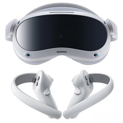
One of the most significant recent developments in LCoS technology is the achievement of extremely high resolutions in compact form factors. Modern LCoS microdisplays can achieve resolutions exceeding 8K in sizes smaller than 0.8 inches, making them ideal for applications such as high-end projectors, augmented reality (AR) headsets, and virtual reality (VR) devices. This high resolution, combined with fast response times, enables incredibly detailed and immersive visual experiences, with smooth cpu lcd screen animations that enhance realism in virtual environments.
Improvements in contrast ratio have been another area of significant progress for LCoS technology. By developing new liquid crystal materials and optimizing the alignment layers, manufacturers have achieved contrast ratios exceeding 1,000,000:1 in some LCoS displays. This is accomplished through better control of light leakage in dark states and improved reflectivity in bright states. These advancements have made LCoS a preferred technology for high-end home theater projectors, where deep blacks and bright highlights are essential for an immersive viewing experience.
Color performance has also seen substantial improvements in recent LCoS developments. The implementation of advanced color filtering techniques and the use of wider gamut color systems have enabled LCoS displays to reproduce a larger percentage of the Rec. 2020 color space, which is the current standard for ultra-high-definition content. This expanded color gamut, combined with improved color accuracy, makes LCoS displays particularly well-suited for professional applications such as color grading, medical imaging, and design visualization, where precise color reproduction is critical.
The integration of LCoS technology with micro-optical systems has opened up new applications in augmented reality and mixed reality. By combining LCoS microdisplays with waveguides and other optical components, manufacturers have created lightweight AR headsets that overlay digital information onto the real world with exceptional clarity. These devices leverage the high resolution and efficiency of LCoS technology to create bright, sharp images that can be viewed even in well-lit environments. The responsive nature of modern LCoS displays also ensures that cpu lcd screen animations and real-time content appear smooth and natural in these mixed reality environments.
Manufacturing advancements have played a crucial role in the commercialization of LCoS technology. The adoption of semiconductor manufacturing techniques has improved yields and reduced costs, making LCoS displays more accessible for a wider range of applications. Additionally, the development of wafer-level packaging has enabled the production of extremely compact LCoS modules with integrated optics, further expanding their potential applications.
Looking forward, the continued development of LCoS technology is focused on increasing resolution further, reducing power consumption, and improving light efficiency. These advancements will enable new applications in areas such as automotive head-up displays, advanced medical imaging, and next-generation AR/VR systems. As LCoS technology continues to mature, it is expected to play an increasingly important role in the display market, particularly in applications requiring high performance in a compact form factor.
LCoS Technology Applications
Home Theater Projectors
VR/AR Headsets
Broadcast Equipment
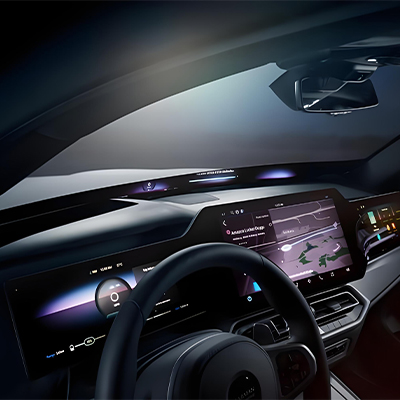
Automotive Displays
Latest LCoS Specifications
Cutting-edge performance metrics