TFT LCD Technology: Core Components and Materials
A comprehensive overview of the essential elements that构成 modern thin-film transistor liquid crystal displays, including insights into quality control and issues like lcd screen white spot phenomena.
1. Glass Substrate
The Glass Substrate forms the fundamental foundation of any TFT LCD display, providing the necessary rigidity and dimensional stability for subsequent layers. These substrates must meet extremely tight tolerances for flatness, thickness, and purity to ensure optimal performance. Typically manufactured from aluminosilicate or borosilicate glass, they undergo rigorous processing to achieve the required specifications.
One critical characteristic of Glass Substrate is its surface quality, as even minor imperfections can propagate through subsequent layers and potentially cause visual defects such as lcd screen white spot formations. Manufacturers employ advanced polishing techniques to achieve near-perfect surface flatness, often measured in nanometers.
Thickness uniformity is another vital parameter for Glass Substrate production. Modern displays utilize substrates ranging from 0.4mm to 0.7mm in thickness, with variations across the panel strictly controlled to prevent optical inconsistencies. This precision helps minimize issues like lcd screen white spot occurrences that can result from uneven pressure distribution during assembly.
Chemical composition of the Glass Substrate is carefully engineered to provide specific properties: high transparency to visible light, resistance to chemical etching processes, and thermal stability during subsequent manufacturing steps. The glass must also exhibit low alkali content to prevent ion migration that could degrade the TFT elements over time.
Manufacturing processes for Glass Substrate typically involve float glass production, where molten glass is poured onto a bath of molten tin, allowing it to form a perfectly flat sheet as it cools. This method ensures the uniform thickness and flatness required for high-quality displays. After forming, the glass undergoes cutting, edge polishing, and thorough cleaning to remove any contaminants that might cause defects like lcd screen white spot in the final product.
Advancements in Glass Substrate technology have enabled the development of flexible displays through the use of ultra-thin glass that can withstand bending without breaking. These innovative substrates maintain the same high standards for purity and surface quality while adding flexibility, though they require special handling to prevent damage that could lead to issues including lcd screen white spot formations.
Quality control for Glass Substrate involves sophisticated inspection systems that can detect microscopic defects. Automated optical inspection (AOI) machines scan each substrate for imperfections that could potentially cause problems in the finished display. Even tiny particles or scratches can lead to issues like lcd screen white spot, making this inspection process critical to maintaining display quality.
Glass Substrate Manufacturing Process
Key Characteristics
Quality Control Focus Areas:
- Surface flatness (< 0.1μm variation)
- Thickness uniformity (< 5% variation)
- Absence of micro-defects
- Chemical purity
- Resistance to thermal stress
- Prevention of potential lcd screen white spot causes
2. Polarizers and Retardation Films
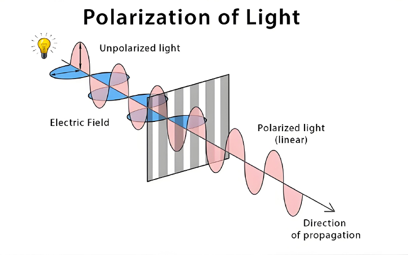
Polarizers and Retardation Films are critical components in TFT LCD technology, responsible for controlling the light waves passing through the display. A typical LCD display incorporates two polarizers positioned perpendicular to each other, with the liquid crystal layer sandwiched between them. These components work in tandem to create the light modulation necessary for image formation.
The primary function of Polarizers and Retardation Films is to convert unpolarized light into linearly polarized light and then control its passage through the display. When light waves encounter a polarizer, only those vibrating in a specific direction are allowed to pass through. The retardation films, also known as phase compensation films, help correct phase differences in light waves, improving viewing angles and reducing color shifts. Proper alignment of these films is crucial, as misalignment can cause optical inconsistencies, including potential lcd screen white spot appearances in certain viewing conditions.
Manufacturing Polarizers and Retardation Films involves complex processes. Polarizers typically consist of a polyvinyl alcohol (PVA) layer sandwiched between protective triacetyl cellulose (TAC) layers. The PVA layer is stretched to align its molecules, then treated with iodine or dye to create the polarizing effect. Any imperfections in this stretching process can lead to uneven polarization, which might manifest as display anomalies including lcd screen white spot in specific circumstances.
Retardation films, a key part of Polarizers and Retardation Films, are engineered to introduce specific phase differences between light waves. These films are crucial for expanding the viewing angles of LCD displays, as they compensate for the birefringence of the liquid crystal layer when viewed off-axis. Advanced retardation films use precisely controlled birefringent materials to achieve optimal performance across all viewing directions, helping to prevent issues like lcd screen white spot that can become more noticeable at extreme viewing angles.
The quality of Polarizers and Retardation Films directly impacts display performance metrics such as contrast ratio, color accuracy, and viewing angle. High-quality polarizers achieve over 99% polarization efficiency while maintaining high light transmittance. Retardation films must provide precise phase compensation values, typically measured in nanometers, with tight tolerances to ensure consistent performance across the display panel. Variations in these properties can lead to visual inconsistencies, including potential lcd screen white spot formations in specific areas.
Anti-glare and anti-reflective coatings are often applied to Polarizers and Retardation Films to improve visibility under various lighting conditions. These coatings use micro-structured surfaces or multi-layer optical films to scatter or interfere with reflected light. While these coatings enhance usability, they must be applied uniformly to prevent creating new optical artifacts that could be mistaken for lcd screen white spot issues.
Environmental durability is another important consideration for Polarizers and Retardation Films. They must resist degradation from moisture, heat, and ultraviolet light to maintain performance over the display's lifetime. Manufacturers use specialized adhesives and protective layers to enhance durability, as delamination or degradation of these films can cause visual defects including lcd screen white spot formations that worsen over time.
Inspection of Polarizers and Retardation Films involves advanced optical testing to verify polarization efficiency, phase retardation values, and freedom from defects. Automated systems check for microscopic imperfections that could affect display quality. Even small defects in these films can lead to visible issues in the final display, such as lcd screen white spot anomalies that become apparent under specific lighting conditions.
Polarizer Structure and Light Polarization
Polarizer Components
- Protective TAC layers
- PVA polarizing layer
- Adhesive layer
- Release film
- Anti-glare coating (optional)
Retardation Film Types
- 1/4 wavelength films
- 1/2 wavelength films
- Positive C-plate
- Negative C-plate
- A-plate and B-plate
Polarization Effect Demonstration
Crossed polarizers demonstrate light blocking effect
3. Backlight Unit
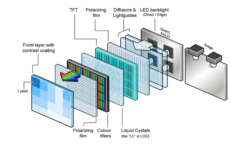
The Backlight Unit (BLU) provides the illumination source for TFT LCD displays, which are inherently non-emissive and require an external light source to produce visible images. The quality of the Backlight Unit directly affects critical display characteristics such as brightness, uniformity, color gamut, and power consumption. A well-designed BLU ensures consistent illumination across the entire display area, preventing issues like uneven brightness that could be mistaken for lcd screen white spot problems.
Modern Backlight Unit designs primarily use light-emitting diodes (LEDs) as the light source, replacing the earlier cold cathode fluorescent lamps (CCFLs). LED backlights offer numerous advantages including lower power consumption, longer lifespan, better color control, and thinner form factors. The LEDs are typically arranged either along the edges of the display (edge-lit design) or in a full array behind the LCD panel (direct-lit design). Each configuration has its trade-offs in terms of thickness, uniformity, and cost, but both require careful engineering to prevent hotspots that might be confused with lcd screen white spot anomalies.
Light guide plates (LGP) are essential components of edge-lit Backlight Unit designs. These transparent acrylic plates distribute light from edge-mounted LEDs across the entire display area through a process of total internal reflection and controlled light extraction. The surface of the LGP features microstructures or printed patterns that extract light in a controlled manner. The precision of these patterns directly affects brightness uniformity; any irregularities can create brightness variations that might be perceived as lcd screen white spot issues in the final display.
Optical films are critical elements within the Backlight Unit, working together to enhance brightness and control light direction. These include: diffuser films that scatter light to improve uniformity, prism sheets (brightness enhancement films) that redirect light toward the viewer to increase on-axis brightness, and reflective films that redirect back-emitted light forward to improve efficiency. The combination and arrangement of these films significantly impact the overall performance of the backlight system. Misalignment or defects in these films can cause optical anomalies, including potential lcd screen white spot appearances in specific areas of the display.
LED drivers are integral to the Backlight Unit, providing precise current control to the LEDs. These drivers include circuitry for dimming control, which can be implemented through pulse-width modulation (PWM) or analog dimming techniques. Advanced backlight systems incorporate local dimming, where different zones of LEDs can be independently controlled to adjust brightness based on image content. This improves contrast ratio but requires sophisticated control algorithms to prevent visible artifacts, including potential lcd screen white spot effects at zone boundaries.
Thermal management is a crucial consideration in Backlight Unit design, particularly for high-brightness displays. LEDs generate heat during operation, and excessive temperature can reduce efficiency, shift color characteristics, and shorten lifespan. The backlight design includes heat sinks, thermal pads, or other cooling mechanisms to dissipate heat effectively. Inadequate thermal management can lead to uneven LED performance across the display, causing brightness or color variations that might be mistaken for lcd screen white spot issues or other defects.
Brightness uniformity is one of the most important performance metrics for a Backlight Unit. Industry standards typically require uniformity above 85% across the display area. Achieving this requires careful design of all components, from LED placement and light guide patterns to optical film selection and arrangement. Any deviation from uniformity can create visible patterns in the display, including areas of increased brightness that might be perceived as lcd screen white spot formations. Manufacturers use sophisticated optical simulation tools during design and automated uniformity testing during production to ensure compliance with specifications.
Color characteristics of the Backlight Unit determine the achievable color gamut of the LCD display. LEDs are available in various color temperatures and spectral distributions, from cool white (high color temperature) to warm white (low color temperature). Some advanced backlights use RGB LEDs to achieve wider color gamuts. The choice of backlight affects color accuracy and consistency across the display. Color variations can sometimes be mistaken for other display issues, including lcd screen white spot problems, making consistent color performance an important quality criterion.
Backlight Unit Structure and Components
Backlight Brightness Distribution
Backlight Unit Types Comparison
| Characteristic | Edge-lit BLU | Direct-lit BLU |
|---|---|---|
| Thickness | Thinner | Thicker |
| Uniformity | Good | Excellent |
| Cost | Lower | Higher |
| Local Dimming | Limited | Advanced |
| Power Efficiency | Good | Very Good |
4. High-Response Liquid Crystal Materials
High-Response Liquid Crystal Materials are the active medium in TFT LCD displays, responsible for modulating light to create images. These unique materials exhibit properties of both liquids and solids, with their molecular orientation controllable by electric fields. The response speed of these materials—how quickly they can change orientation in response to an electric field—is critical for display performance, particularly in fast-moving content like video games or action movies. The chemical composition and physical properties of High-Response Liquid Crystal Materials are carefully engineered to balance multiple performance parameters while maintaining stability and reliability.
Molecular structure is a key determinant of the properties of High-Response Liquid Crystal Materials. Most LCD materials consist of rod-shaped organic molecules that naturally align parallel to each other. This anisotropic structure gives them unique optical properties—their refractive index varies depending on the direction of light propagation relative to the molecular orientation. When an electric field is applied, these molecules reorient, changing the optical properties of the material. This electro-optical effect forms the basis of LCD operation. Any impurities or inconsistencies in these materials can lead to display defects, including potential lcd screen white spot formations in specific areas.
Response time is a critical performance metric for High-Response Liquid Crystal Materials, typically measured as the time required for the material to transition between light and dark states. Modern displays require response times in the millisecond or even sub-millisecond range to prevent motion blur in fast-moving content. Achieving this requires careful molecular design and mixture formulation. The rotational viscosity of the liquid crystal material is inversely related to response speed—lower viscosity enables faster response. However, viscosity must be balanced with other properties like stability and operating voltage. Impurities that increase viscosity can lead to uneven response across the display, potentially creating artifacts that might be mistaken for lcd screen white spot issues during rapid image transitions.
Dielectric anisotropy is another important property of High-Response Liquid Crystal Materials, describing how their dielectric constant varies with molecular orientation. Positive dielectric anisotropy materials align with electric fields, while negative dielectric anisotropy materials align perpendicular to them. This property determines the operating mode and voltage requirements of the LCD. Materials with higher dielectric anisotropy can operate at lower voltages, reducing power consumption. The uniformity of this property across the display is crucial, as variations can cause uneven brightness or contrast that might manifest as lcd screen white spot anomalies in specific regions.
Refractive index anisotropy (birefringence) of High-Response Liquid Crystal Materials determines their light-modulating efficiency. This property, combined with the cell gap (thickness of the liquid crystal layer), determines the optical path difference that creates the light or dark states. Precise control of both the material's birefringence and the cell gap is necessary to achieve optimal contrast ratios. Variations in birefringence across the display can lead to inconsistent optical performance, including potential lcd screen white spot appearances in areas where the balance between material properties and cell gap is disrupted.
Operating temperature range is a critical consideration for High-Response Liquid Crystal Materials, as their properties can vary significantly with temperature. Displays must function reliably from cold (-20°C or lower) to hot (60°C or higher) conditions depending on their application. Liquid crystal materials are formulated to maintain stable properties across this range, with minimal changes in response time, viscosity, or optical characteristics. Temperature-induced variations can cause temporary or permanent display issues, including potential lcd screen white spot formations in extreme conditions if the material properties are not properly stabilized.
Chemical stability is essential for High-Response Liquid Crystal Materials to ensure long-term reliability. These materials must resist degradation from exposure to light, heat, and electric fields over the display's lifetime (typically 50,000 hours or more). Degradation can lead to changes in optical properties, increased response time, or even permanent display defects. Stabilizers are often added to liquid crystal mixtures to enhance their resistance to degradation. Material breakdown in localized areas can cause permanent lcd screen white spot formations that do not disappear with changes in displayed content.
Modern High-Response Liquid Crystal Materials are typically mixtures of multiple liquid crystal compounds, each contributing specific properties to the overall performance. Formulating these mixtures is a complex process that balances response speed, operating voltage, temperature stability, and other characteristics. Advanced mixtures may include chiral dopants to induce specific molecular twist structures or other additives to modify properties. The uniformity of these mixtures is critical, as any separation or concentration variations can lead to display inconsistencies, including potential lcd screen white spot anomalies in areas where the mixture composition varies.
Quality control for High-Response Liquid Crystal Materials involves rigorous testing of both individual compounds and final mixtures. Parameters measured include refractive indices, dielectric constants, viscosity, response time, and stability under various conditions. Even trace impurities can significantly affect performance, making high-purity standards (typically 99.9% or higher) essential. Automated inspection systems check for contaminants that could cause defects like lcd screen white spot in the finished display, ensuring only materials meeting strict specifications are used in production.
Liquid Crystal Behavior and Response Characteristics
Response Time Comparison (ms)
Key Liquid Crystal Properties
- Rotational viscosity
- Dielectric anisotropy
- Refractive index anisotropy
- Clearing point (phase transition)
- Elastic constants
Common LCD Operation Modes
- Twisted Nematic (TN)
- In-Plane Switching (IPS)
- Vertical Alignment (VA)
- Advanced Super View (ASV)
- Optically Compensated Bend (OCB)
Note: Liquid crystal response time is temperature-dependent, with slower response in cold conditions and faster response at higher temperatures. This can affect display performance in extreme environments and potentially contribute to artifacts resembling lcd screen white spot in certain conditions.
5. Driver and Control IC/LSI Manufacturing Process
The Driver and Control IC/LSI Manufacturing Process produces the specialized integrated circuits that control the operation of TFT LCD displays. These chips manage the complex functions required to render images, including signal processing, timing control, and individual pixel addressing. The Driver and Control IC/LSI Manufacturing Process combines advanced semiconductor fabrication techniques with display-specific design optimizations to create chips that deliver high performance while minimizing power consumption and cost. The reliability of these components is critical, as failures can cause various display anomalies, including potential lcd screen white spot patterns in affected areas.
Design is the first stage of the Driver and Control IC/LSI Manufacturing Process, involving the creation of circuit schematics and layouts tailored for display applications. These designs must address specific requirements such as resolution, refresh rate, color depth, and interface standards. Modern driver ICs integrate multiple functions including timing controllers, data drivers, gate drivers, and power management circuits. Designers use advanced EDA (Electronic Design Automation) tools to optimize for performance, power efficiency, and manufacturability. Simulation tools verify functionality before fabrication, checking for potential issues that could cause display defects like lcd screen white spot patterns in specific operating conditions.
Wafer fabrication is a critical phase in the Driver and Control IC/LSI Manufacturing Process. This involves creating multiple ICs on a single silicon wafer through a series of photolithography, etching, deposition, and doping steps. The process begins with a polished silicon wafer, which undergoes cleaning to remove any contaminants. Photolithography transfers circuit patterns onto the wafer using light-sensitive materials (photoresists) and masks. Etching removes material in specific areas to form trenches and vias, while deposition processes add conductive, insulating, and semiconductor materials in precise locations. Doping introduces impurities to modify the electrical properties of silicon regions, creating transistors and other active components. The precision of these processes directly affects IC performance, with any variations potentially leading to inconsistent display operation, including possible lcd screen white spot formations in specific pixel regions.
Transistor fabrication is a key aspect of the Driver and Control IC/LSI Manufacturing Process. Most modern display driver ICs use complementary metal-oxide-semiconductor (CMOS) technology, which combines both n-type and p-type metal-oxide-semiconductor field-effect transistors (MOSFETs). The transistor gate length is a critical technology node, with smaller nodes enabling higher integration density and lower power consumption. Advanced driver ICs use process technologies down to 28nm or smaller, allowing for more functionality in a smaller die area. The uniformity of transistor characteristics across the wafer is essential, as variations can lead to inconsistent signal timing or voltage levels that might cause display artifacts including lcd screen white spot patterns in specific areas.
Wafer testing is performed after fabrication in the Driver and Control IC/LSI Manufacturing Process, where each die on the wafer is tested for functionality and performance. Automated test equipment (ATE) applies test patterns and measures responses to identify defective dies, which are marked for exclusion during packaging. Tests verify parameters such as operating voltage range, signal timing, data processing accuracy, and thermal performance. This screening process is critical for ensuring only functional ICs proceed to the next stage, preventing potential display issues including lcd screen white spot problems caused by IC malfunctions.
Packaging is an important stage in the Driver and Control IC/LSI Manufacturing Process, protecting the delicate silicon die and providing electrical connections to the outside world. Display driver ICs often use specialized packaging techniques to accommodate the large number of input/output connections required while minimizing size. These include Chip-on-Glass (COG), where the IC is directly bonded to the display glass, and Tape Carrier Package (TCP), where the IC is mounted on a flexible tape with conductive leads. Advanced packaging technologies like Fan-Out Wafer-Level Packaging (FOWLP) are also used to achieve smaller form factors with improved electrical performance. The reliability of these packaging techniques is crucial, as poor connections can cause intermittent or permanent display issues, including potential lcd screen white spot patterns in areas controlled by the affected connections.
Final testing completes the Driver and Control IC/LSI Manufacturing Process, verifying the performance of packaged ICs under various conditions. This includes functional testing at different temperatures and voltage levels to ensure reliability across the operating range. Burn-in testing may be performed, where ICs are operated at elevated temperatures and voltages for an extended period to identify early-life failures. The data from these tests helps characterize IC performance and ensure compatibility with specific display modules. Any ICs that fail to meet specifications are rejected to prevent integration into displays, where they could cause issues like lcd screen white spot anomalies or more severe display malfunctions.
Advanced features in modern driver ICs, produced through the Driver and Control IC/LSI Manufacturing Process, include built-in self-test capabilities, adaptive brightness control, and advanced image processing functions. These features enhance display performance and enable diagnostic capabilities that can help identify issues like lcd screen white spot causes. Some driver ICs include temperature sensors and compensation circuits to maintain consistent performance across operating conditions. The integration of these advanced features requires increasingly sophisticated manufacturing processes and testing procedures to ensure reliability and performance.
Quality control throughout the Driver and Control IC/LSI Manufacturing Process is essential for ensuring display reliability. Statistical process control (SPC) techniques monitor critical manufacturing parameters to maintain consistency and identify process variations before they affect product quality. Traceability systems track each IC from design through manufacturing, enabling targeted improvements and rapid root cause analysis for any issues that arise. This comprehensive quality approach helps minimize display defects, including those that manifest as lcd screen white spot anomalies, by ensuring the driver and control ICs perform consistently across all operating conditions.
Driver IC Manufacturing Flow and Integration
IC Integration Technologies
Key Functions of LCD Driver ICs
- Timing control and synchronization
- Data signal processing and conversion
- Gate and source voltage generation
- Power management and regulation
- Image enhancement algorithms
- Defect compensation (including lcd screen white spot mitigation)
- Temperature compensation
- Interface with host system
Integration and Quality Assurance
The performance of a TFT LCD display depends on the precise integration of all components described above. Each element—from the Glass Substrate to the Driver and Control IC/LSI—must meet stringent quality standards to ensure optimal performance and reliability.
Quality control processes throughout the manufacturing chain are essential for minimizing defects such as lcd screen white spot formations. Advanced inspection technologies, including automated optical inspection, electrical testing, and environmental stress testing, help identify potential issues at each production stage.
Continuous advancements in each component area—improved Glass Substrate materials, more efficient Polarizers and Retardation Films, brighter and more uniform Backlight Unit designs, faster High-Response Liquid Crystal Materials, and more sophisticated Driver and Control IC/LSI solutions—continue to drive the performance improvements seen in modern TFT LCD displays.